My first PCB
Schematic and Layout
Table of Contents
Introduction
This isn't my first time designing a PCB and soldering it. Quite the opposite to what is stated in title, right?
During my schooldays at the HTL (technical school) we were taught how to draw a schematic in Eagle, create the layout and export the Gerber files. In the end, these PCBs were milled directly in the school.
While that sounds great and I definitely learned something, it mostly was copy pasting step for step. If you didn't mess up throughout, your design was sure to work at the end.
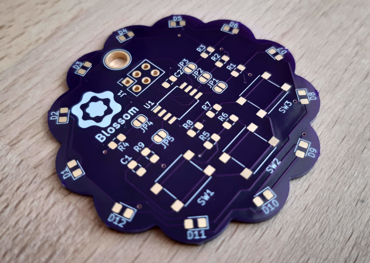
This time I wanted to do it all on my own, doing my own project where it is not sure from the start that everything will work out, and where I am allowed to screw up. That's what I did here: I designed a nice little PCB that also doesn't look too bad aesthetically. The PCB is called blossom because the board outline resembles a flower - maybe you can see it?
But lets start at the beginning. I wanted to design the board with Open Source Software, therefore KiCad was the way to go.
The repository for the board can be found at blossom-kicad.
The Schematic
My requirements were simple: I wanted to blink some LEDs and press some buttons. The whole thing should be powered by a cell battery and weigh little enough to have it hanging around your neck (that requirement was easy to fulfill).
I have already had some experience with the ATtiny Series, that's why I decided on the ATtiny85.
Among the ATtinys, the ATtiny85 is the one with more capabilities, concerning Flash (8K Bytes), EEPROM (512 Bytes) and RAM (512 Bytes) but still a fun programming challenge. I opted for the ATtiny85V-10SU which is slower (10 MHz instead of 20 MHz) but works at lower voltages (down to 1.8V).
Have a look at my guide for the ATtiny85.
Now, we have 6 Pins available as two pins are used for supply voltage and ground. What unimaginable things can we do with them?
The Reset Pin
One of the pins is the reset pin with an internal pull up resistor. It's quite weak with R_RST = 30 kΩ - 60 kΩ but strong enough for me to not bother with an external pull up.
In the documentation it is also stated, that the reset pin can be used as an I/O pin:
The reset pin can also be used as a (weak) I/O pin.
In order to do that you need to set the RSTDISBL Fuse Bit which disables the reset pin as a reset. But once the reset is disabled you need a high voltage programmer to reprogram the uC. Because I will often reflash the uC and don't own such a programmer I will leave the reset pin as it is.
The Remaining Pins
5 Pins left. With four of them I want to control some LEDs. The last remaining pin will then be used as an input.
Charlieplexing
Charlieplexing is used to drive LEDs with relatively few I/O pins. Just four pins can control up two 12 LEDs!
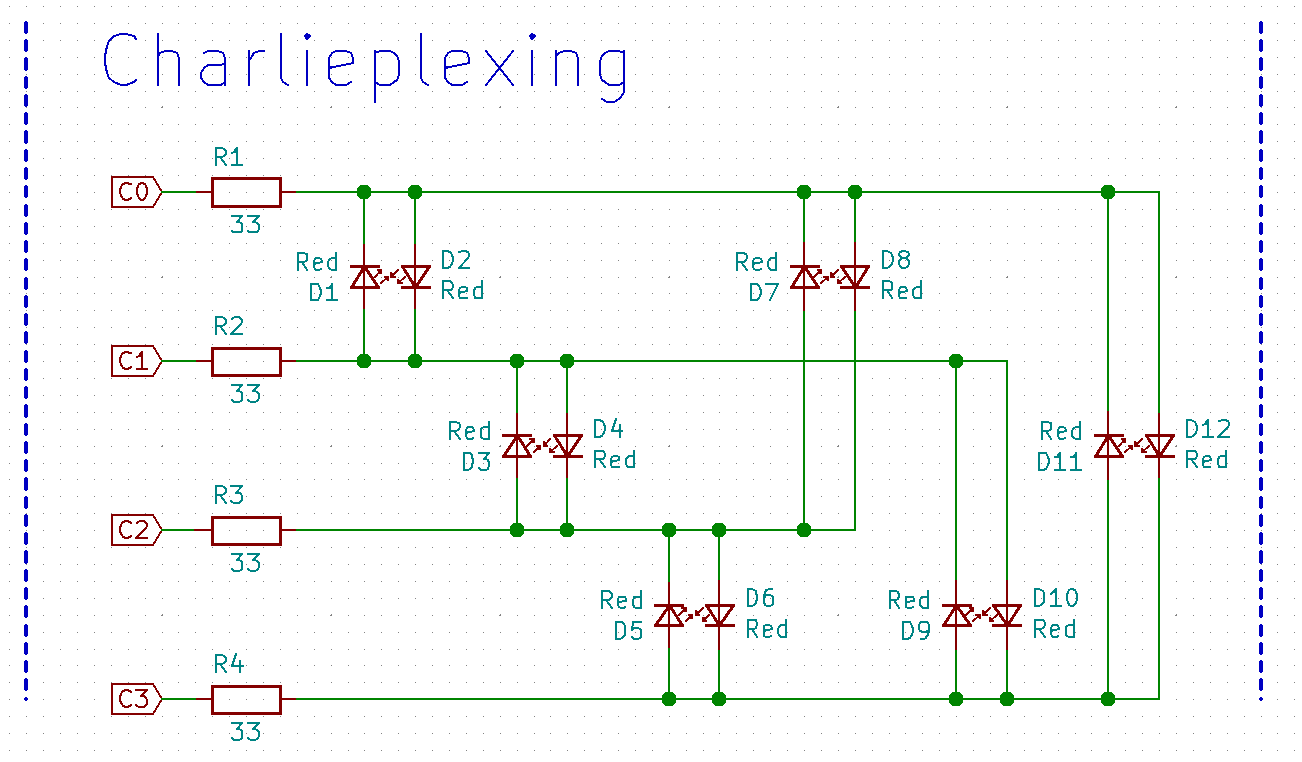
The trick here is to only have two pins set as output at once. The rest of the pins is set to input (high-impedance) and won't affect the circuit. Then one of the two output pins will be set to High and the other one to Low resulting in lighting one LED.
For example:
- Set C0 and C1 as output
- Set C2 and C3 as input
- Set C0 to High and C1 to Low
The LED marked as D2 will light up.
With a method called multiplexing we can make it seem like all LEDs light up at once. This is done by controlling one LED after another, but doing it so fast that our eyes are tricked into thinking that all are lit at once.
An that's all there is to say.
Analog Input
The last pin can be used as an analog input. I had an idea how to take advantage of that: 3 buttons that when pressed charge up a capacitor (for debouncing) with different voltage levels. I can then read the voltage and infer which buttons were pressed. Maybe even multiple button presses at once can be registered?
There is one problem, I want to use a simple CR2032 cell battery to power the whole design and voltage divider would continuously consume energy. Therefore I need to make the resistors as big as possible. But the bigger the resistors the longer it takes to charge the capacitor. Just make the capacitor smaller you say. But then we would have a huge error when measuring the voltage as the capacitor of the sample-and-hold stage of the ADC is similar in size.
The middle way it is:
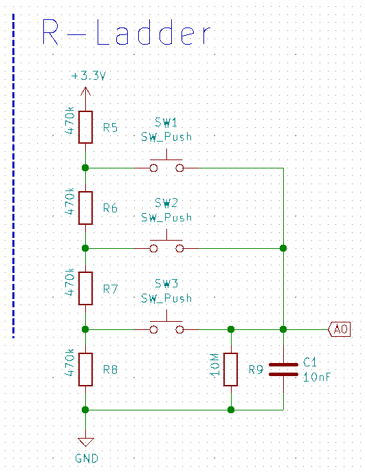
I have chosen the capacitor C1 as 10 nF, therefore it is still much bigger than the capacitor of the sample and hold stage (14 pF) thus reducing the error.
Now we only have to decide on the resistors in the R-ladder. The path of the greatest resistance is open when SW3 is closed: In this case there is a resistance of 3*470 kΩ.
With the RC time constant called tau we can calculate how long it takes to charge the capacitor:
tau = R * C = 3 * 470 kΩ * 10 nF = 14.1 ms
After 5 times tau the capacitor is almost charged up (~99 %) this results in a charging time of 70.5 ms. Discharging happens over R9 with 10 MΩ taking half a second.
Simulations have shown reasonable results. Let's see how that will perform in reality.
Layout
Now comes the fun part. Layouting the whole design.
Board Outline
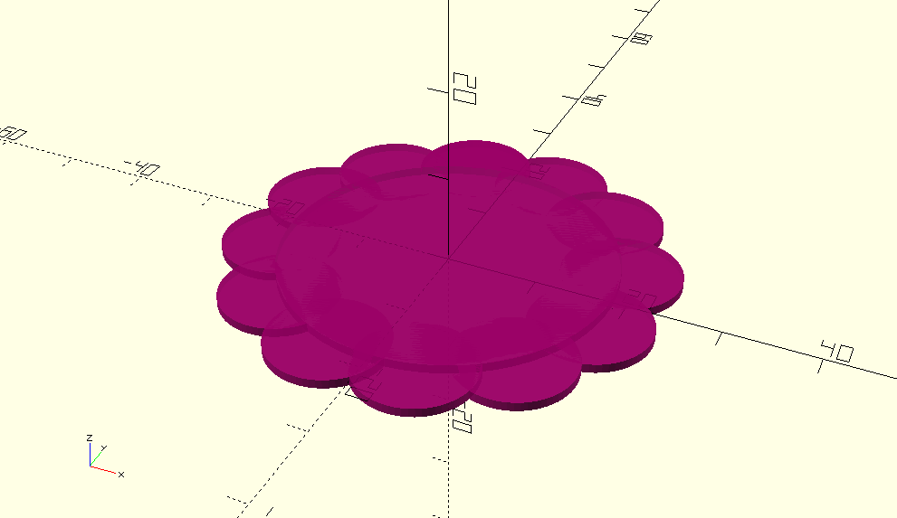
I wanted my board outline to be exact, that's why I used OpenSCAD to programatically create a board outline, drill holes and positions that can than be used to align the LEDs more easily.
I can only recommend this workflow.
Placing the Components
First I placed the uC in the middle, the buttons where I want to have them, the cell battery holder on the back of the PCB and the LEDs at the edges with the positions I have exported from OpenSCAD.
I wasn't sure if my programmer can both program the ATtiny and supply enough current for whatever the ATtiny is doing at the moment (lighting LEDs). Because I have not found a definitive answer to that question I decided to place some open solderbridges between the ATtiny and the components. I would then program the ATtiny and afterwards close the solder bridges.
You can read in the next post whether this was really necessary (hint: it was not).
Designing Footprints
Because there was no footprint available for the battery holder that I was going to buy I had to design my own. I have always been afraid of that: Just always use parts that are in the standard library and you are good to go. What happens if you didn't get the dimension right and aren't able to solder the component? Gruesome thoughts.
But in that case I really had to bite the bullet. But as you can see it didn't turn out that bad:
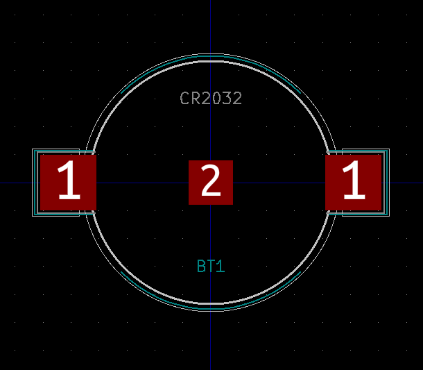
From now on I will not be afraid of designing my own footprints.
Routing
Now comes the part where we are actually connecting the components:
Pressing x in the PCB Layout Editor lets you add a track. Pressing v while laying a track places a via and automatically changes to the other side of the board.
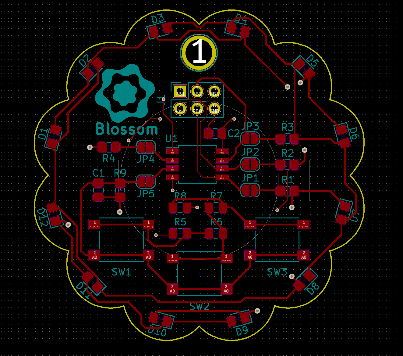
Quite tight at the edges, but enough space everywhere else. I think I can easily reduce the size next time.
And now?
I decided to have my boards fabricated at OSH Park - definitely not because I like their nice purple solder masks, nooo that was definitely not why I chose them...
Also OSH Park lets you directly upload a KiCad PCB as if you had provided the Gerber files. Very convenient.
Fabrication took around a week, but shipping took far longer. You can read about why that didn't matter in the next article in the series: here.